IMPLEMENTATION OF CONTINUOUS TIME DELTA SIGMA BASED RF ANALOG TO DIGITAL BAND PASS CONVERTER FOR LTE RECEIVER
By
Sai Varrshini Macha Venkata
U1345673
A dissertation submitted in partial fulfilment
of the requirements for the degree of:
Master of Science
in
Electrical & Electronics Engineering
Submitted to the University of East London
On
22 May 2015
Supervisor: Dr.Jaswinder Lota
Abstract
Long Term Evolution (LTE) is the effective communication technology
that provides outstanding customer experience by offering high data rates with
good response time. A number of researches are being carried out to develop different
architecture’s to improve the system, because of the increase in demand for the
LTE communication.
The main objective of this project work is to design,
develop, analyse and check with the theoretical and simulation results for
continuous time delta sigma analog to digital converters that operate for LTE
specifications.
This study discusses the LTE specifications as specified by
ETSI, sets out the front end requirements for LTE receiver and does the
theoretical calculation of dynamic range of the system which is then quantified
with the simulation results of the system level design. The study extends to
exploring the challenges involved in circuit level implementation and also
discusses the differences between the continuous time and discrete time
modulators.
System level design is built using SIMULINK and the model is
simulated with MATLAB software. The theoretical and simulation results are
quantified with the help of the example design. The various methods have been
proposed to improve the system results and the results are analysed for varying
the parameters.Acknowledgements
I would like to thank, the almighty for blessing me with
good health and mental strength towards the completion of my work.
The study could not have been completed without the
guidelines provided by my project supervisor Dr Jaswinder Lota, Senior
Lecturer, University of East London. I am really grateful to my project
supervisor for his immense contribution of ideas and his valuable suggestions helped
me to complete the work.
I wish to express my
thanks to all my friends, tutors and lab assistants in University of East
London, who have been really helpful in the accomplishment of this work. I owe
a special thanks to OpenAthens login account, which helped me to refer various
IEEE journals at my convenience, which made valuable contribution to the study.
I wish to express profound thanks to entire staff and
management of 'University of East London’ for providing me with uninterrupted
lab facility and library support without which it would have been impossible to
complete this work.
Finally, I am thankful to my entire family, for the
encouragement and constant support throughout the completion of the course.
Acronyms
Term
|
Definition
|
ADC
|
Analog to Digital Converter
|
DSM
|
Delta Sigma Modulator
|
CT
|
Continuous Time
|
DT
|
Discrete Time
|
SNR
|
Signal to Noise ratio
|
OSR
|
Over Sampling Ratio
|
ACI
|
Adjacent Channel Interference
|
LNA
|
Low Noise Amplifier
|
VGA
|
Variable Gain Amplifier
|
LTE
|
Long term Evolution
|
BW
|
Band Width
|
BS
|
Base Station
|
DR
|
Dynamic Range
|
ETSI
|
European Telecommunication Standards Institute
|
GSM
|
Global System for Mobile communication
|
AGC
|
Automatic Gain Control
|
RF
|
Radio Frequency
|
PAPR
|
Peak Average Power Ratio
|
DAC
|
Digital to Analog Converter
|
LSB
|
Lowest Significant Bit
|
NRZ
|
Non Return to Zero
|
HRZ
|
Half return to zero
|
RZ
|
Return to zero
|
IIT
|
Impulse Invariant Transformation
|
PSD
|
Power Spectral Density
|
NTF
|
Noise Transfer Function
|
LF
|
Loop Filter
|
STF
|
Signal Transfer Function
|
FIR
|
Finite Impulse Response
|
DEM
|
Dynamic Element Mismatch
|
List of Tables
1 Introduction
Wireless communication has become the recent necessity
throughout the world. It is expected to grow more with the further increase in
demand. One of the main reasons for this development has been identified by Thandri,
(2006) is because of the major improvement in radio frequency circuit design.
The speed of wireless communication is the important parameter which depends on
the applied standards. There are various researches currently under study to
improve the speed of wireless communication. This paper concentrates with the
LTE standard of communication. The major aim of this paper is to explore
various design techniques to implement ADC system and the system level design
for a continuous time band pass delta sigma ADC for LTE receiver is carried
out. Finally, the dynamic range requirements from theoretical calculation and
simulation results are quantified.
1.1 Aims and Objectives
The aim and objectives of this study is listed below:
- To study the front end requirements for LTE receiver.
- To mathematically calculate the dynamic range for the LTE specifications specified.
- To explore the types of delta sigma modulators in use and to study the differences between CT and DT DSM.
- To quantify the dynamic range requirements with the practical implementation of the design.
- To explore the circuit level challenges involved in implementing the design.
- To analyse the results obtained and to discuss the variation in dynamic range for varying certain parameters.
1.2 Paper Organisation
Chapter 1 introduces the wireless communication needs, lists
the aims and objectives of the study.
Chapter 2 defines the front end requirements for RF receiver;
the specifications defined in the LTE standards are discussed. Later in the
chapter the dynamic range for LTE standards are mathematically calculated.
Chapter 3 presents the theory of delta sigma ADC, lists the
differences between CT DSM and DT DSM and concludes with the reason for
selecting CT ∆∑ ADC system.
Chapter 4 reviews the methods to improve the dynamic range
of the system and concludes with the parameters considered for this design.
Chapter 5 explains in detail about the design description
and the step by step procedure to calculate the loop filter coefficients.
Chapter 6 presents the difficulties involved in implementing
CT DSM.
Chapter 7 explains the method involved in generating
Simulink model and the Matlab script which controls the entire simulation is
described. Later in this chapter, the results are analysed by varying the order
of the system and number of bits in quantizer.
Chapter 8 summarises the conclusions of the study and presents
the future work that can be carried with this paper.
Chapter 9 contains lists of references that were used in
this paper.
Chapter 10 lists the additional sources that were referred
to gain clarity of concepts to complete this work.
Chapter 11 Appendix – contains the source code of
implemented CT DSM system and the specification of the band pass filter.
2 Quantifying Dynamic Range Requirements
2.1 Front end
There are several specifications that need to be taken into
consideration while designing the front end of the wireless receiver. Rofougaran et al., (1996) considered sensitivity of
the front end to be the most important feature when designing. To maintain the
receiver sensitivity, the front end gain must be kept high enough to overcome
the later stage noise contributions. The input noise of the front-end must be
sufficiently low to enable it to detect weak input signals.
1.2 Reference Sensitivity Level
Reference sensitivity level is defined as:
“The reference sensitivity power level is the minimum mean
power received at the antenna at which a throughput requirement shall be met
for a specified reference measurement channel”
- ETSI
Standards TS 136 104 V9.4.0. (2010, p.46)
The reference sensitivity level for various types of base
stations for the LTE bandwidth range from the ETSI LTE standards is presented
in the Table 1.
Bandwidth
|
Wide area BS
|
Local area BS
|
Home BS
|
BW
|
Rs
|
Rs
|
Rs
|
1.4
|
-106.8
|
-98.8
|
-98.8
|
3
|
-103
|
-95
|
-95
|
5
|
-101.5
|
-93.5
|
-93.5
|
10
|
-101.5
|
-93.5
|
-93.5
|
15
|
-101.5
|
-93.5
|
-93.5
|
20
|
-101.5
|
-93.5
|
-93.5
|
(Source: ETSI Standards, 2010)
The lowest sensitivity level is found to be -106.8 and the
highest bandwidth available from the ETSI LTE standards is 20 dB. The system is designed for these particular
specifications.
2.3 Dynamic Range
The dynamic range can be defined as:
“A measure of the capability of the receiver to receive a
wanted signal in the presence of an interfering signal inside the received
channel bandwidth”
- ETSI Standards TS 136 104 V9.4.0. (2010)
Dynamic range can be mathematically written as:
DR = Pmax- (Rs-10)
|
In this equation (1), because of the CT∆∑ ADC circuit non
ideologies, where clock jitter and thermal noise plays a role, the dynamic
range value is obtained by subtracting the sensitivity level with 10 dB for the
ease in physical implementation.
2.4 Interference’s
2.4.1 In channel Selectivity
In-channel selectivity (ICS) can be defined as:
“A measure of the receiver ability to receive a wanted
signal at its assigned resource block locations in the presence of an
interfering signal received at a larger power spectral density”.
- ETSI Standards TS 136 104 V9.4.0. (2010, p.49)
2.4.2 Adjacent Channel Selectivity
Adjacent channel selectivity (ACS) can be defined as:
“A measure of the receiver ability to receive a wanted signal
at its assigned channel frequency in the presence of an adjacent channel signal
with a specified centre frequency offset of the interfering signal to the band
edge of a victim system”.
- ETSI Standards TS 136 104 V9.4.0. (2010, p.51)
2.5 LTE Specifications
Onet et al., (2014) summarised the
specifications for the LTE operating range in the Table 2.
Standard
|
Operation frequency [GHz]
|
Channel bandwidth (BW) [MHz]
|
Minimum sensitivity [dBm]
|
Maximum input level [dBm]
|
|
LTE
|
0.7 to 3.8
|
1.4; 3; 5; 10; 15; 20
|
-106.2 – 101.7 @BW-1.4 MHz
|
-94 / -91 @BW-20MHz
|
-25
|
(Source: ETSI Standards, 2010)
The centre frequency for the operating band is specified in
the ETSI Standards TS 136 104 V9.4.0. (2010) and is presented in the Table 3.
E-UTRA Operating Band
|
Uplink operating band frequency
|
20
|
832 MHz – 862 MHz
|
(Source: ETSI Standards, 2010)
2.6 Low Noise Amplifier (LNA)
In the RF receiver front end, LNA is the first and most
challenging block. LNA provides gain which suppresses the noise to improve the
system selectivity and sensitivity. Tuan and Farrell,
(2010) experimentally obtained maximum power gain, which ranges from 13
to 17 dB for different bands with controlled range of over 15dB. The LNA gain
can be controlled over different ranges for multimode operation.
Rodriguez et al., (2014) experiments
showed the gain of the LNA is around 14 dB with a 3dB bandwidth of 6GHz.
2.6.1 LNA Specifications
Marzuki, Abdul Rahim and Loulou,
(2012) summarised the specifications for LNA, which is tabulated in the Table 4.
Specification
|
Optimum Range
|
Optimum point
|
Gain (dB)
|
10 to 20
|
20
|
NF (dB)
|
1 to 6
|
1
|
IIP3 (dBm)
|
-5 to 5
|
5
|
Based on the experiments, the range of LNA’s gain varies
around 13 - 17 dB. Therefore, the
average value 15 dB is chosen for
the front end design.
2.7 Variable Gain Amplifier (VGA)
VGA is the next block prior to the Analog-to-Digital
converter (ADC).VGA’s linearity and bandwidth depends on the gain settings.
Most often, the VGA bandwidth is not controlled and its value is kept large, to
avoid substantial impact on its characteristics. But, the VGA gain is
controlled because of the two reasons, it can employ a section of the channel
filter and it also restricts the noise bandwidth based on the channel
bandwidth. Usually, the gain is adjusted in several large steps combined with
finer gain steps or even continuous gain control. Based on the time window
permitted by the communication standards, step-like gain adjustments are
implemented. Experimental results shows that the gain can be varied between 5 dB to 30 dB in three gain ranges,
with wide overlaps (Onet et al., 2014).
The minimum and maximum gain of VGA is chosen as 5dB and 30
dB respectively for RF front end implementation of CT∆∑ BP ADC modulator.
The dynamic range of the front end is calculated based on
the signal power level and the adjacent channel interference level.
2.8 Case 1: Power > Adjacent Channel Interference (ACI)
The dynamic range value for the signal power level greater
than the ACI is calculated using the equation (1). In this equation, Pmax
denotes the maximum power of a signal at the ∆∑ ADC input. The value of Pmax
goes through variations because of the peak average power ratio (PAPR) and
fading. The reference sensitivity level (Rs) and bandwidth is chosen as -106.8
dBm and 20 dB respectively from the LTE specifications.
ETSI TS GSM 05.05 Version 5.0.0 (1996) specified that the
transmitting power for GSM base stations vary from 20W - 40W in an urban
environment, although the standards specify even higher power levels of 80W.
Mann et al., (2000) have experimentally proved that at a
distance of 20m from an 80W base station, the radiation power levels
would be at most +30 dBm. The transmission powers for LTE are similar to GSM (3
GPP Technical Standard 3GPP TS 25.101 v6.12.0 (2006-06) Technical
Specification).
The LNA block’s gain is assumed as +15 dB. VGA with AGC is
able to keep the maximum level of the signal (Pmax) to a an
intermediate value despite the combined effects of RF filtering, fading and
peak-to average power ratio (PAPR).Variable gain amplifier can offer up to 5 to
30 dB which keeps the Pmax to about -45 dBm.
Therefore, based on the fixed specifications, the dynamic
range is calculated as:
DR = -45 – (106.8 – 10) = 71.8 dB
|
(2)
|
2.9 Case 2: Power < ACI
When the interference level is greater than signal power,
the receiver is detecting the minimum detectable signal against strong
interference. The signal power and the adjacent channel interference level for
the LTE bandwidth range as specified in the ETSI Standards TS 136 104 V9.4.0. (2010)
is summarised in the Table 5.
BW
|
Signal mean power [dBm]
|
Interfering signal mean power [dBm]
|
Interfering signal centre frequency offset from the
channel edge of the wanted signal [MHz]
|
Type of interfering signal
|
1.4
|
Rs+11 dB
|
-52
|
0.7025
|
1.4MHz E-UTRA signal
|
3
|
Rs+8 dB
|
-52
|
1.5075
|
3MHz E-UTRA signal
|
5
|
Rs+6 dB
|
-52
|
2.5025
|
5MHz E-UTRA signal
|
10
|
Rs+6 dB
|
-52
|
2.5075
|
5MHz E-UTRA signal
|
15
|
Rs+6 dB
|
-52
|
2.5125
|
5MHz E-UTRA signal
|
20
|
Rs+6 dB
|
-52
|
2.5025
|
5MHz E-UTRA signal
|
(Source: ETSI Standards, 2010)
The adjacent channel specifications require the minimum detectable
signal to be 6dB above Rs for 20 MHz BW from the
Table 5.
Lowest reference sensitivity level (Rs) -106.8 dBm and highest bandwidth
available is chosen from LTE specs.
2.9.1 Calculating Pmax for LTE
The signal power for the chosen bandwidth (20) is now,
Rs+6 dB = -106.8 + 6
= -100.8 dBm.
After passing through the RF filter, it is assumed that
there is some insertion loss, 3 dB. Now the signal power (P1) becomes,
P1 = -100.8 + 3 = -97.8 dBm.
LNA gives a fixed gain of +15 dB and VGA adjusts itself to
its maximum +30dB.Therefore, Pmax is now calculated as,
Pmax = -97.8+15+30 = -52.8 dBm
-52. 8 dBm is the maximum power obtained in this case.
2.9.2 Calculating Pmax for Blocker
The interfering signal mean power of LTE for 20 bandwidth
signal is found out to be -52 dBm. The blocker performance requirements from the ETSI
specifications are tabulated in Table 6.
Operating Band
|
Centre Frequency [MHz]
|
Interfering signal mean power [dBm]
|
20
|
(FUL_low -11) to (FUL_high +20)
|
-43
|
(Source: ETSI Standards, 2010)
The filter response for the BAND PASS FILTER FB-0860
designed by Marki microwave is shown in the Figure
1.


(Source: Marki Microwave, 2012)
The band pass filter response shows that the insertion loss
will be zero. LNA gives a fixed gain of +15 dB and VGA adjusts itself to its
maximum +30 dB. Therefore Pmax is calculated as,
Pmax = (-52.8+15+30) = 7 dBm.
|
Band pass filter response
 |
The values from both the signals are summarised in Table 7
and dynamic range is calculated by taking the difference between the two
values.
|
Antenna
|

3 Delta Sigma ADC
The swift in the market for the portable devices indicated the
inclination towards the digital domain in VLSI systems. The evolution of the
handy and battery operated systems in communication devices and electronics
resulted in the shift of analog to digital systems. The change in the market
trend brought out huge interest in analog to digital converter (ADC) over the
last few years (Ortmanns and Gerfers, 2006).
The A/ D converter can be designed in many possible ways
depending on the system’s speed and resolution. The most widely preferred
conversion design is ∆∑ ADC. ∆∑ Method is chosen because of its low
sensitivity to the circuit non ideologies. The conventional ADC’s are extremely
sensitive to circuit deficiencies and they need correction mechanisms to avoid
them. This is eliminated in the ∆∑ ADC with the use of digital signal post
processing (Ortmanns and Gerfers, 2006).
The increase in the need for
higher bandwidth systems in the telecommunications sector brought out the need
for architectural choices. In this design, continuous time ∆∑ modulators are
implemented rather than the discrete time modulators because of their settling
time constraints. In the continuous time modulators, the entire loop filter is
built in continuous-time circuits (Ortmanns and
Gerfers, 2006).
Cherry and Snelgrove, (2000) have
listed the basic components for analog to
digital conversion as,
- A loop filter or loop transfer function H (z).
- A clocked quantizer.
- A feedback digital to analog converter (DAC).
3.1 Principle
of Continuous Time Delta Sigma ADC
The major difference in the continuous time modulator design
is that the sampling is done before the quantisation. Cherry
and Snelgrove, (2000) have mentioned in his research work that the loop filter
is built with continuous time circuits in this type of delta sigma ADC. The
continuous time loop filters widely used are RC or gm/C or LC integrators. The
noise shaping technique and oversampling property are the same in both CT and
DT systems. Gupta, (2015) experiments
have concluded that the feedback DAC is implemented with a current-steering DAC
for continuous time circuits.
The input signal is passed through
the loop filter before sampling, where the loop filter itself acts as an anti-aliasing
filter, thus eliminating the need for external anti-aliasing filter. The system
order depends on the level of anti-aliasing achieved. The CT converter doesn’t
need a switching load to the input because of moving the sampler away from the input
which eases the bandwidth specifications. As the continuous time system
doesn’t need a switching load, it helps to reduce the power consumption and
they also do not have stringent settling requirements (Cherry
and Snelgrove, 2000). The trend towards development of CT systems increased
because of their various advantages over DT such as in-built anti-aliasing
filter, reduction in power consumption, and decrease in the noise power
(Andersson, 2014). Some of the important advantages and disadvantages of CT
system over DT modulator is presented by Kulchycki (2008) are listed below.
3.1.1 Advantages
- The need for external anti-aliasing filter is eliminated, as the loop filter itself acts as its anti-aliasing filter.
- Low power consumption compared to DT equivalent.
- Low supply voltage is enough for its operation.
- Can operate at high sampling frequency.
- High bandwidth requirements are achieved.
3.1.2 Disadvantages
- Discrete time modulators are used for precision dc-type application.
- CT system cannot modify the modulator’s sampling period as required by the system, which makes it inappropriate to use for dc type applications.
3.2 Principle
of Discrete Time Delta Sigma ADC
Andersson, (2014), have explained in
his experiments that the discrete time delta sigma modulator consists of loop
filter, ADC and feedback DAC which is similar to the CT modulator. The major
difference being that the sampling of the input signal is done before the loop
filter operation in DT system. Gupta, (2015), has summarised the operating
parameters of the DT system as follows: loop filter is implemented using
switched-capacitor integrators, quantizer is set up to be of low resolution,
feedback DAC is implemented using switched-capacitor technique. The
quantization noise is shaped up by the loop filter which moves away the noise
from the baseband region. A decimation filter is used in addition in the DT
system which filter’s the quantizer’s output at the low pass region.
Even though DT system provide higher
resolution, they are not preferred because of the problems involved such as
charge injection, clock feed through and need for sample and hold circuit at
the front (Chae, 2013).
3.3 Why CT ∆∑ ADC is chosen over DT ∆∑ ADC
The possible general reasons for choosing the CT ∆∑ ADC over the DT ∆∑ ADC has been listed by Cherry and Snelgrove, (2000).
- In general DT ∆∑ ADC has a fixed clock sample which is restricted by the operational amplifier bandwidth, whereas, in a CT ∆∑ ADC there is no restriction in the bandwidth thus the circuit waveforms vary continuously. Theoretically, it is concluded that the order can be increased with ease in the CT modulator.
- The switching transients in the DT modulator, results in the hitches in the op amp virtual ground nodes, which is absent in CT modulator. One of its applications is (dS90), where 20-bit resolution is achieved. In this example, the converter stages were made up of CT circuit.
- The major issue with the DT modulator system operation is the requirement of external aliasing filter which is not the case in CT modulator where the loop filter itself acts as an anti-aliasing filter. DT ∆∑ ADC requires an external filter to weaken the aliasing property of the system.
- CT modulators can be used basically wherever a DT modulator is used.
- These reasons make continuous time design to be an efficient architecture choice for this study.
4 Achieving High Dynamic Range
The value of dynamic range of the system can be increased by
varying various factors. The change in the value of SNR with the change in the
parameters is explained in the following section.
4.1 Signal to Noise Ratio
The signal-to-noise ratio is obtained by dividing the signal
amplitude frequency by the root mean square of all frequencies representing
noise which for an N-bit ADC is mathematically represented as in equation (3),
(3)
|
The empirical formula for SNR is given in equation (4) as,
(4)
|
Therefore, from the equations above, SNR is a function of
three parameters namely,
- Order (L)
- Over Sampling Ratio (OSR)
- Number of quantizer bits (B)
If the signal to noise ratio is improved, the quality and
the accuracy of the digitized signal will be improved and the noise level will
decrease. The dynamic range of an ADC is restricted by the quantization noise.
The quantization error is defined as:
“The “round-off” error that occurs when an analog signal is
quantized”
-
Anon, (2015)
4.1.1 Changing the Number of Quantizer Bits
While converting a signal from analog to digital, the output
will have only fixed points unlike the input signal with infinite points.
Therefore the output will not fully replicate the input analog waveform. The
quantisation of digital output gives rise to a difference of about ½ LSB
between the input and output signal. The amount of quantization uncertainty can
be reduced if the number of bits is increased, thus reducing the quantization
noise level. Though the increase in number of bits increases the SNR, one
cannot keep on increasing it because of the technical constraints and limitations.
4.1.1.1 Limitation
The practical conditions restrict the matching accuracy of
electronic components to about 0.02%; hence N is restricted to about 12 bits.
4.1.2 Changing the Oversampling Ratio
As the number of bits cannot be increased to any value to
increase the SNR, because of the constraints, the sampling frequency can be
increased by an oversampling ratio. The practice where the analog input signal
is sampled at a frequency greater than the Nyquist frequency is called
Oversampling. The sampling frequency is now OSR x fs instead of fs. By
increasing the sampling frequency, the noise floor will be dropped.
This process decreases the quantization noise in the bandwidth
required. This means that increasing fs will decrease the
noise by 9 dB in the required band (Anon, 2015).
Though the process of oversampling reduces noise in the converter, this
reduction is even greater for delta-sigma modulators, which increases the SNR.
“The SNR improves by 3 dB, or 0.5 bit, each time the sampling
frequency is doubled”
-
(Loloee, 2013)
The noise energy will be spread over the wider frequency
range and this noise can now be easily filtered when passed through a digital
filter. Thus the root mean square noise is reduced, thereby increasing the SNR.
There is no change in the signal power as it occurs over the signal band. The
signal-to-noise ratio as defined by Reiss, (n.d) may
now be given by the equation (5)
PreviousSNR+10log10OSR
|
(5)
|
The ADC can achieve high resolution, by increasing the OSR
value to higher value, which requires high sampling rates. The implementation
of noise shaping technique can overcome this situation by bringing in an increase
in gain of about 6dB for each factor of 4 OSR.
‘Oversampling rate’ is defined as:
“Due to the sampling theorem the sampling rate must be higher
than twice the maximum input frequency. Any further increase is called
oversampling rate”.
-
Beis.de, (2015)
Beis.de, (2015) have explained the
concept of OSR in detail in the example below:
“Example: Assume an audio signal with a bandwidth of up to 20
kHz. A typical sampling rate (for DAT etc.) is 48 kHz. In a typical delta sigma
converter the clock frequency will be 64 x 48 kHz = 3072 kHz. This is equal to
an oversampling rate of 64. Here, the clock frequency is 64 times higher than
the frequency of the input signal. This means that the oversampling rate must
be less than 32 for the given input frequency”.
-
Beis.de, (2015)
4.1.3 Changing the Order
The integrator in the 1st order ∆∑ modulator acts
as a low pass filter to the input signal and a high pass filter to the
quantization noise, thus shaping the noise. When digital filter is applied for
the noise shaped output, it removes more noise than oversampling technique. The
1st order ∆∑ modulator provides an overall improvement of 9 dB in
SNR. If the order of integration is changed from 1st to 2nd
order, it can provide an improvement of 15 dB in SNR. Thus increasing the order
of integration increases the SNR which in turn provides higher effective number
of bits giving a better ADC resolution.
Beis.de, (2015) have explained this
concept as; the noise produced by the bit streams from the higher order
modulator is much lower than the lower order modulator. The main disadvantage of
the 1st order modulators is that there are some strong
frequencies in the power spectrum.
The change in the value of SNR, for changing the OSR by two
times the previous OSR can be calculated from equation,
3(2L + 1)dB
|
(6)
|
Loloee, (2013) have summarised the
increase in the SNR with the increase in the order of the modulator in the Table 8.
Order
|
OSR
|
SNR improvement in dB
|
1st
|
2
|
9 dB
|
2nd
|
2
|
15 dB
|
There is an increase in about 6 dB in the SNR value, for a
change in the order of the modulator.
Anon, (2015) plots the relationship
between the SNR and OSR for a 1st, 2nd and 3rd
order modulators is shown in the Figure 3.


(Source: Anon, 2015)
It can be understood from the graph that the increase in the
oversampling ratio and the order of the modulator, increases the SNR linearly.
The Figure 4
shows the quantization noise spectrum of Nyquist type converter and the theoretical
representation of SNR.

(Source: Anon, 2015)
The Figure 5
shows the graphical representation of oversampled converters, with the spread
out noise. Thus the quantisation noise in the band of interest is reduced,
whereas the total noise remains the same.


(Source: Anon, 2015)
The Figure 6
demonstrates the noise shaping of the oversampled DSM, where the total
quantization noise is still the same but the in-band quantization noise is
greatly reduced.


(Source: Anon, 2015)
Reiss, (n.d.) has summarised the
overall relationship between the OSR, order and SNR improvement of the
modulator as:
“For an Nth order SDM, there is a 3(2N+1) dB improvement in
the SNR with each doubling of the oversampling ratio, and a 3dB improvement
with each additional bit in the quantizer. Thus, use of high order SDM's and a
high oversampling ratio offers a much better SNR than simply increasing the
number of bits”.
-
Reiss, (n.d.)
4.2 Design Consideration
The parameters that can be varied for achieving higher
dynamic range was discussed in the previous section and the parameters that
have been considered for the system level design is described in the following
section.
- The number of bits (B) is generally limited to 2-3 bits. Here it is restricted to 2 bits.
- Oversampling ratio is fixed to 32 because of the power consumption problem.
- Oversampling ratio = Sampling frequency / Nyquist frequency = Fs= 32 / 2*20 = 1.28 GHz.
- The order is restricted to 2nd order.
The signal to noise ratio can be calculated using the equations
(7) and (8) below.
SNR = 73.664 (after substituting B=2, L=2, OSR= 32)
73.664 = 6.02N + 1.76
71.90 = 6.02N
N = 11.9 bits.
The
ADC resolution of about 11 bits is achieved with the parameters considered for
designing, in spite of restricting the no of bits to 2. The OSR, L, B change is
applicable to only low pass filter. Conventionally, the band pass filter can be
implemented, by replacing z by z*z. And the order becomes 4 from 2. Therefore,
first the system is designed as low pass filter and then the frequency transformation is done to achieve band pass
filter system.
5 Architectural Design
The system level simulation model is built for the desired
bandwidth and frequency range with the pre-selected oversampling ratio, number
of bits and order. Schreier and Temes, (2005) has explained that the outline
design for discrete time system are more established than the continuous time
design and hence therefore the first step in designing will be to obtain a
discrete time design for the preferred results. The entire process of designing
is done with the help of MATLAB toolbox.
5.1 Design Description
Delta sigma modulator usually consists of following blocks:
- Loop filter
- ADC
- Feedback DAC
The block diagram for CT DSM and DT DSM is shown below:


(Source: Zheng, Mohanty, Kougianos, 2012)
5.1.1 Loop filter
The loop filter is usually integrators in case of low pass
filters, which are replaced with tank circuits for the design of band pass
filter systems. In this design, as the system order is chosen to be 4 for
achieving better dynamic range results, 2 tank circuits are used in linear
fashion. The tank circuits are constructed with second order continuous time
coefficients. There are various types of tank circuits available which is
chosen according to the design specification. LC tank circuits are selected for
this design which acts as band pass filter. LC tank circuit is selected instead
of SC tank circuit because of its implementation in continuous time system. The
LC tank circuit works like a resonator which is used for tuning the radio
transmitters and receivers.
5.1.1.1 LC tank Circuit
The LC tank circuit is the first and foremost block that is
to be considered while designing DSM. The general LC tank circuit is shown in
the Figure 8.

(Source: Ashry, Aboushady, 2010)
The designing of LC tank circuit involves selecting values
for the inductor (L) and capacitor (C).
According to Thandri, (2006) experiment’s
the value of L is chosen based on its geometry and to enhance the quality
factor at its centre frequency. Niknejad and Meyer,
(1998) experiment’s proved that the quality factor and the value of the
inductors depends on the numerous
factors such as shape of the inductor, number of turns in the coil, thickness,
conductivity and resistivity of the material.
“The IBM 0.25 µm
SiGe technology offers custom inductors with a pre-determined shape on metal layers
and some variable parameters (number of turns, distance between metal turns,
hollowness etc.) that are restricted to a certain range of values”.
-
Thandri, (2006)
These restrictions
controls the design of the inductors and the Q factor of the inductor is
limited for the target application’s centre frequency that occupies minimum
area. Thandri (2006) research proposal has chosen the value of inductor to be
5.1 nH. This value, results in the maximum Q factor for the centre frequency.
“The topmost metal
layer is used in order to minimize the capacitance between the metal and the
substrate. A mesh layer is used to shield the spiral inductor from the
substrate, which increases the resistivity of the substrate beneath the spiral
and decreases the inductor losses”.
-
Thandri, (2006)
The parasitic capacitance
is chosen to be around 110fF. The area occupied by the shunt capacitance comes
with no extra penalty.
In this design for
LTE’s centre frequency, the value of capacitance is calculated using the
formula
.
5.1.2 ADC
The output from the loop filter, which is the loop filter
coefficients, goes through the ADC as an input to the modulator. This analog
signal is then converted to digital output by ADC. The digital output is then
fed back into the loop filter. The loop filter shapes the quantisation noise.
This way delta sigma modulator acts as an ADC. Noise shaping happens because of
the presence of two components: STF and NTF. As presented in (Chang, 2009) thesis, noise shaping converters can be
classified into following types: single-bit single-loop low-order designs, single-bit
single-loop high order designs, multi-loop cascaded designs with feed-forward
error cancellation, and multi-bit noise shapers. The most commonly used type is
single–bit high-order designs because of the ease in the implementation and
simplicity. ADC acts as a quantizer and the quantizer can be either single-bit
or multi bit based on the target application design. The single bit
quantizer is selected for the DSM aimed for LTE centre frequency. ∆∑ Modulators
can be implemented either in CT or DT techniques. Because of the various
advantages, CT technique modulator is preferred for this design.
5.1.3 Feedback DAC
The output from the ADC modulator is fed into the DAC, which
converts back the digital signal to analog signal. This analog signal is again
fed back into the loop filter which helps to shape away quantisation noise.
Therefore, feedback DAC pulse is an important design consideration for
designing this system. The type of feedback DAC used must be chosen with utmost
care. The different types of DAC pulse gives different loop coefficients when
applying impulse invariant technique. The various types of DAC pulses that are
available are: NRZ DAC pulse, HRZ DAC pulse and RZ DAC pulse.
5.1.3.1 NRZ DAC
The change in the polarity of the comparator output ignites
the change in the DAC pulse transition. That is the DAC pulse change over from
the high to low or vice-versa. Thandri, (2006)
have mentioned in his research work that when there is no change in the
polarity, the earlier value of the bit stream will be maintained in a NRZ DAC
pulse for that clock cycle.
5.1.3.2 RZ DAC
The RZ DAC pulse has the low or high value of the bit for
half a clock period and returns to zero value for the other half of the clock
period (Thandri, 2006).
5.1.3.3 HRZ DAC
The HRZ DAC pulse exhibits the same behaviour as RZ pulse
with the difference that it is shifted in time by ½ of the clock period
(Thandri, 2006).


(Source: Thandri, 2006)
The NRZ DAC pulse is chosen for this particular design
application after comparing the advantages and disadvantages of all types of
DAC pulse. In addition to this, compensation DAC pulse is also used in case of
excess loop delay.
5.1.3.4 Compensation DAC
The feedback DAC will not be sufficient to counterpart the
continuous time loop gain and the discrete time loop gain. This results in the
excess loop delay, which will be compensated by the addition of the
compensation DAC. Ashry, Aboushady, (2010) documented that the CT to DT
conversion, is used to find out the loop gain for the compensation branch. The
CT to DT conversion is easier to implement in this case, because of the
presence of the feedback DAC in the compensation branch.
5.2 Discrete time system design
The discrete time system is designed for the specified
bandwidth and dynamic range requirement using MATLAB toolbox with various
factors such as modulator order, oversampling ratio and out-of-band gain. Discrete
time loop gain function is found to satisfy the requirements. Conventionally, the
low pass filter discrete system is designed and converted to band pass through
frequency transformation. Then the band pass CT system is then converted to
band pass DT system through impulse invariant transformation. But, this study
is implemented by using band pass filter at the initial stages.
5.2.1 Impulse invariant Transformation
Impulse invariant technique is widely used for designing
discrete time impulse response system. This transformation can be done
mathematically, by performing partial fraction expansion and Z transform for
the analog transfer function. Mathematical transformation is a time consuming
process which is now replaced with the transformation done with the help of
MATLAB. The syntax for performing the impulse invariant transformation is as
follows:
[numd,dend] = impinvar (num,den,fs) (9)
The impulse invariant method of transformation is selected
instead of bilinear transformation mainly because of its ease in implementation
and the accurate plotting of results.
5.2.2 Calculating Loop Transfer function
The loop transfer function usually consists of two parts:
signal transfer function (STF) and noise transfer function (NTF). Zheng, P.
Mohanty and Kougianos, (n.d.) have considered the STF to be unity. Therefore
the noise transfer function has to be found, to obtain LF. The NTF and LF
coefficients are mathematically related as:
(10)
|
The noise transfer function can be obtained by using the
Schreier’s Delta sigma toolbox which has the inbuilt functions such as
synthesize NTF, thus avoiding the tedious manual process. The synthesize
function needs parameters such as OSR, order, OBG to produce NTF. The syntax
for using the synthesize function and the NTF for the specified parameters are
obtained as shown below.
SynthesizeNTF (Order, OSR, Opt, H-inf, f0)
|
(11)
|
Where the order indicates modulator design order, OSR is the
oversampling ratio selected, Opt indicates flag for optimized zeros, H-inf
indicates maximum NTF gain and Fo is the centre frequency. The noise
transfer function with substituted parameters is shown below.
ntf=synthesizeNTF(4,32,0,1.5,0.25)
|
(12)
|
Therefore, NTF obtained is
(z^2 + 1)^2
-------------------------------------------------
(z^2 -
0.3222z + 0.6645) (z^2 + 0.3222z + 0.6645)
The impulse response of all the integrators of the
continuous time has to be found. The LC tank filter’s loop filter coefficients
for each node is found.
5.2.3 DT coefficients calculation
The DT equivalent model’s loop gain using impulse invariant
technique can be found using the equation:
Gct(z) = Z{L-1[H(s)HDAC(s)]}
|
(13)
|
(Source: Ashry & Aboushady, 2010)
The conversion from continuous time to discrete time can be
done easily with the command ‘c2d’. The syntax for using c2d command is
Sysd = C2d(sys, Ts, method or opts)
|
(14)
|
Here,
Gct = c2d(Hs2, Ts,‘zoh’)
|
(15)
|
Gct equation discretizes the continuous time system using
zero order hold on the inputs and a sample of Ts specified.
When converting from CT to DT ‘zoh’ command is used for the
NRZ DAC pulse. It also implies that the impulse invariant transformation is
implemented. Each LC tank filter circuit has a FIR feedback gain which is added
between the output and the feedback DAC which can be represented mathematically
as:
GDT (z) = GCT (z)*F
(z)
|
(16)
|
(Source: Ashry &
Aboushady, 2010)
The continuous time system’s loop transfer and the discrete
time’s loop transfer function have the same denominator therefore only the
numerator value has to be matched. This relation can be represented in matrix
form as:
[bDT] = [bCT]*[f]
|
(17)
|
(Source: Ashry &
Aboushady, 2010)
where, bDT
and bCT represents the numerator elements of the
continuous time and the discrete time system. Therefore the matrix coefficients
can be calculated by taking out the inverse of the CT transfer function, which
can be represented mathematically as,
[f] = [bCT]-1*[bDT]
|
(18)
|
(Source: Ashry &
Aboushady, 2010)
The overall loop filter coefficient can be calculated as
follows:
GDT (Z) = Loop Gain of first loop filter *
Feedback + Loop Gain of 2nd loop filter * Feedback + Loop gain of
Compensation feedback.
The resultant value can be used to compute the matrix
coefficients.
6 Circuit level Challenges
The non- ideologies of the circuit is the key parameter that
has to be considered while designing an analog to digital converter. The
circuit will perform to its full capacity when the non-ideologies are
minimized. The effect of each of the non-ideologies are explained in the below
sections. The various type of non-ideologies of circuit are clock jitter,
comparator meta stability, loop delay, Q-factor, unequal DAC pulse rise and
fall, dynamic element mismatching, multi-level high speed DAC. These
non-ideologies reduce the quantization noise’s transfer function which
decreases the effective SNR of the ADC. They also result in the loss of
stability of the system (Thandri, 2006).
6.1 Clock Jitter
The performance of the system depends on the clock’s
sampling quality. Clock jitter can be explained as the ambiguity in the time
instant at which ADC signal are sampled. This results in the increase in the
noise which reduces the overall system performance.
According to Thandri, (2006) research experiments, the clock
signal may differ from its ideal behaviour and it is called as clock jitter.
The clock jitter’s deviation is reproduced as noise in the ADC output; this
noise is added to the noise floor.
“The power of the error term depends on the rms value of
clock jitter. The error term due to NRZ is much lower than the error term due
to RZ/HRZ DAC”
-
Thandri, (2006)
The analog to digital converter that
samples at a higher rate is more prone to the clocking issues and results in
the significant distortion. They have also mentioned that oversampling the ADC
is predicted to improve this condition. In ∑∆ modulator, oversampling is
expected to improve the value of SNR in spite of the clock jitter degradation (Poornima, Trivedi and Dipti Lal, 2009).
6.2 Loop delay
The feedback path’s restricted switching time of transistors
gives rise to the delay in the DAC current pulse ideal response and the delay
is called as excess loop delay. This is represented in the form of delay block
after the loop filter transfer function in the block diagram. The noise floor
degrades with the increase in the loop delay and leads to the SNR degradation.
The excess loop delay leads to the increase in the order which in turn leads to
the stability issues and it can be solved by adjusting the loop filter coefficients
or by decreasing the out-of-band gain of noise transfer function (Thandri,
2006).
The diagrammatical representation of the deviation from the
ideal response is shown in the figure below.


(Source: Thandri, 2006)
The increase in excess loop delay will also affect the phase
response of the filter. The analysis with a 3rd order ∆∑ ADC have
shown that the phase response decreases whereas the amplitude remains unchanged
and concluded that the loop delay and stability depends on the design of ADC (Cherry and Snelgrove, 2000)
Cherry and Snelgrove, (1999) have
mentioned that excess loop delay is because of the following reason.
“The DAC currents respond
immediately to the quantizer clock edge, but in practice, the transistors in
the latch and the DAC have a nonzero switching time. Thus, there exists a delay
between the quantizer clock and DAC current pulse, and we call this delay
excess loop delay.
-
Cherry and Snelgrove,
(1999)
They have also suggested some
techniques to avoid the excess loop delay:
- By carefully selecting the DAC Pulse
- Proper tuning of feedback coefficients
- With the inclusion of additional feedback parameters
6.3 Q-factor
The LC tank circuit acts as a loop filter for the 4th
order continuous time ∆∑ ADC. The LC tank circuit has associated losses with
them, which is represented in the form of resistor. The fundamental
representation of Q factor as defined in the Thandri, (2006) research work is
shown in the equation (19) where Q represents the amount of losses present in
the system.
(19)
|
The Q factor of LC tank circuit can be found using the
equation (20),
(20)
|
The Q factor is found to be directly related to the inductor
losses. The Q factor of the band pass filter affects the noise transfer
function of the modulator. For higher values of Q, the noise floor reduces
which increases the SNR. The Q factor of LC tank circuit can be improved by
adding a negative resistance (-R) in parallel to the existing resistance (Rs),
so that it can cancel out the losses caused by the Rs (Lota and Demosthenous, 2015).
The selection of inductor with high Q
factor will not be a good choice, as it may not provide expected results. The
inductor selection also depends on various other factors such as number of
turns, layout and transfer function of the system. The ∆∑ ADC modulator is
simulated for various values of Q factor and the dynamic range for each system
is analysed.
The graphical representation of change
in the noise transfer function with the Q factor is shown in the Figure 11.

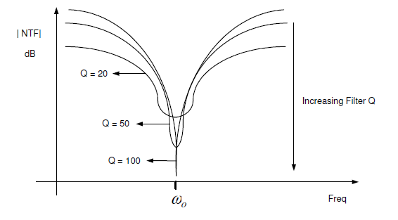
(Source: Thandri, 2006)
6.4 Dynamic Element Mismatch
“The one-bit
delta-sigma modulation has its ability to achieve arbitrarily high linearity. A
multi-bit DAC cannot be made perfectly linear since it is impossible to create
a transfer characteristic with steps of exactly equal height. Since non-ideologies
in the DAC are equivalent to noise added directly to the input signal, DAC
errors can easily be the performance-limiting factor in a delta-sigma ADC or
DAC”.
- Lin et.,al (1996)
Lin et. al (1996) have also mentioned in his publication
that multi bit converter exhibits higher modulator performance and increases
the resolution. Though multi bit modulator offers higher performance, it is not
preferred widely because of the problems caused by excessive loop delay, higher
power dissipation and DEM.
The multi bit ∆∑ converter has a component
value deviation error, and it was conventionally eliminated by trimming the
digital to analog elements or by randomizing the error. The trimming technique
was found to be expensive and it is now replaced with dynamic element mismatch
technique. DEM digital to analog converters effectively eliminates the element
mismatch in the system.
6.4.1 Principle of Dynamic Element Mismatch
The dynamic element mismatch technique reduces the deviation
by varying the components interconnection.
“These algorithms rearrange the interconnections of
mismatched components so that the time averages of the equivalent components at
each of the component positions are nearly equal. If the mismatched components’
virtual positions are appropriately varied, the harmonic distortion caused by
the mismatched components can be reduced, frequency shifted or eliminated. As a
result, DEM algorithms can increase an ADC’s SFDR, SDR, SNDR and ENOB”.
-
Wayne Bruce (2000)
According to Wayne Bruce, (2000), research,
various methods exist in DEM algorithm implementation:
- Deterministic DEM algorithm.
- Stochastic DEM algorithm.
- Digital DEM algorithms.
The digital DEM algorithm is most widely used for the multi-bit
ADC converter implementation.
7 Simulation – Results & Discussion
During the course of the process, the simulations are
performed to ensure that the requirements are met. The entire process is
controlled by the MATLAB script. The continuous time delta sigma model can be
constructed using signal processing toolbox in the Simulink and the output
power spectral density is plotted using the toolbox. The SNR value can be
calculated from the plots. The Simulink has various in-built libraries which
are used to build the blocks such as integrators, gain, net sum, quantizer’s
etc. The delta sigma modulator’s interactive model can be built with Simulink.
The Simulink model of the CT DSM is shown in the Figure 12
(Zheng, P. Mohanty and Kougianos, n.d.)
7.1 Simulink model
Simulink is in-built tool with the MATLAB, which is used to
model, simulate and analyse systems. There are various customised libraries
present which are used to represent dynamic systems. The blocks are then built
representing the loop filter, feedback DAC, gain, quantizer and saturation. The
sine wave input signal is used as the reference analog input signal which is
then converted to digital signal. The
loop filter block is constructed for 2nd order system, which is
represented as,
. The system is chosen to be a 4th order
system, therefore two 2nd order loop filter is used in the linear
fashion. The gain coefficients are named as gm1 and gm2. The 3 input port
summer precedes the loop filter, which is used to sum up the feedback signal
with the incoming signal. The feedback DAC’s gain coefficients are named as a1,
a2, a3, a4 and a5. The zero order hold sampler is used to perform the sampling
function. It also represents that the DT to CT conversion is performed by the
impulse invariant transformation. The sampler is followed by the quantizer
block, where the quantizer interval can be varied. The variation in the
quantizer interval represents the level of the quantizer. A saturation block is
used after the quantizer, where the upper limit and lower limit of the input
signal can be limited. A delay is used in the feedback path, to decrease the
meta-stability problem as mentioned by Thandri, (2006). The output at any point
of the system can be viewed with the help of scope option.


7.2 Matlab Script
A MATLAB script is written, which is used to control the
performance of the system. The Simulink model is then synchronised with the
MATLAB script. The initialisation of parameters and the calculation of the
dynamic range from the plots are explained in the following sections.
7.2.1 Initialising the parameters
The analog to digital converter is designed for the centre
frequency of 832 MHz and a bandwidth of 20 dB, which are the LTE receiver’s
specifications. Therefore, the centre frequency (fc) is assigned to 832 MHz
and the sampling frequency is 1/4th of the centre frequency. As
discussed in the section 5.1.1.1,
the inductor value (L) is initialised to be of 5.1nH. The value of the
capacitor is calculated using the expression,
(21)
|
According to Thandri, (2006), the gain coefficient, gm1,
converts the input voltage to current, which is fed back into the loop, and the
DR is calculated using this value. The second filter gain coefficient, gm2
value, is chosen taking into consideration of power consumption, noise
etc. The gm1 is assigned the value of
100/1000 and gm2 is assigned to be of 4/1000. The values obtained for the
capacitor and A are given in the Figure 13.

7.2.2 Generating noise transfer function
The noise transfer function has to be found before moving on
to the calculation of loop transfer function. The in-built synthesizeNTF
function from the delta sigma toolbox is used to generate the NTF using the
loop filter order. The obtained noise transfer function will be in the zeros
and poles format which is then converted to transfer function using ‘zp2tf’
command. The loop filter calculation is done using the numerator and
denominator coefficients of NTF. The loop transfer function is then converted
to z-1 convention.
The screenshots showing the generation of noise transfer
function and loop coefficients are shown in the Figure 14.


The Q factor and its value selection as described in section
6.3
are taken into account while designing the Q factor of LC tank circuit. The Q
factor is initially assumed to be 100 and then the value is varied to obtain
the results which are then compared and analysed. The loop filter function’s
coefficient is calculated using the expression (22) & (23),
(22)
|
||
(23)
|
7.2.3 Generating Loop filter coefficients
The calculation of loop filter coefficients for each block
is calculated by writing the transfer function in the numerator and denominator
format. The transfer function, Hs2, is written by considering the two loop
filter blocks. The value of ‘A’ in the numerator is substituted with w02L.
The transfer function for Hs3 is written with only one loop filter block.
The obtained transfer function is then converted from continuous to discrete
system using ‘c2d’ command. The transfer function obtained from Hs2
and Hs3
are named as N1 and N2 respectively. These transfer function are then written
in the matrix format and named as B. The matrix D is then formed by taking the
inverse of matrix B and then multiplied with transfer function obtained from
NTF. The filter coefficients are then obtained from the matrix. The loop filter
coefficients obtained are presented in the Figure 16,
Figure 17,
Figure 18,
Figure 19
& Figure 20.


The Simulink block is now simulated by specifying the
simulation time and the power spectral density is now plotted.
7.2.4 Plots
The power spectral density for the 4th order
system is then plotted and is shown in the Figure 21.
It can be seen from the figure that it shows good noise shaping concentrating
at the centre frequency (832 MHz).

7.2.5 Calculating the dynamic range
The signal to noise ratio can be calculated from the power
spectral density plot by zooming in the plot by considering the bandwidth
region around the centre frequency. The calculation of SNR is explained
diagrammatically in the Figure 22.
|
Y (Max signal power)
|
|
822 MHz
|
|
832 MHz
|
|
842 MHz
|
|
X(Max noise
power)
|
|
20 dB
|
The maximum signal power measured is marked as Y, and the signals
at ±10 dB from centre frequency, i.e., 822 (832-10) and 842(832+10) is noted.
Within the specified bandwidth region, plot the highest noise signal as X.
Then, the SNR value can be calculated using the expression (24),
(24)
|
Therefore,
The plot showing the calculation for the dynamic range is shown in
the figure below.

The dynamic range for the plot above with Q = 100 is
calculated as 73.93 dB from the simulation results.
7.3 Achieving high DR by varying Q factor
The selection of Q factor is an important parameter that
must be considered while designing a system. As discussed in section 6.3,
increasing the Q factor increases the SNR. The plots are then generated for
various values of Q and the results are analysed. The plot for Q = 100 is
generated and the dynamic range is measured. Then the value of Q factor is
changed from 100 to 150 and then it is simulated again. In the same manner, the
Q-factor can be changed to any value and the results are summarized in the Table 9.


Q-factor
|
SNR (dB)
|
100
|
73.9
|
150
|
74.63
|
200
|
77.82
|
7.3.1 Graphical representation
The graphs representing the noise shaping for Q = 100, 150 and 200
is shown in the figure below.

7.4 Achieving high DR by varying the quantizer levels
As discussed in section 4.1.1,
the dynamic range of the system increases as the number of bits increases. The
use of multi-bit quantizers does not behave non-linearly as single bit
quantizer, thus improving the stability of the system and improves the noise
transfer function (Yan and Sanchez-Sinencio, 2004).
Marques et al., (1998) have explained in his research that the improvement in
noise shaping for multi bit quantizers gives an improvement in dynamic range of
the system as compared with single bit quantizer.
Though multi bit quantizers have
various advantages, it is not widely preferred to increase the number of bits
to higher value because of the loop delay problem, which is explained in
section 6.2. The number of bits of the quantizer can be
varied by changing the quantizer interval of the quantizer block in Simulink
model. The dynamic range of the system with variation in the number of bits are
analysed in the sections below.
The screenshots showing the change in
the quantizer interval is shown in Figure 28,
Figure 31
& Figure 34.
7.4.1 2-level quantizer
The system is initially simulated with quantizer interval
set to 1 and the results are plotted. The dynamic range is then calculated from
the plots for single bit quantizer. The
single bit quantizer is also called as a 2-level quantizer. The diagrammatical
representation of 2 levels is shown in Figure 27
below.
|
0
|
|
1
|

In the same manner, the value of Q-factor is varied for different
values and the increase in SNR is plotted in the Figure 29
and the results are summarised in Table 10.

Q-factor
|
SNR
|
70
|
72
|
90
|
72.96
|
110
|
72.65
|
130
|
77.97
|
7.4.2 4-level quantizer
The quantizer interval is now changed from 1 to 0.5, which
gives a 4 level quantisation. The results from the graph is analysed and it is
noted that there is an improvement in the dynamic range of the system. The 2
bit quantizer is shown in the Figure 30.

(Source: Hodgson, Jay 2010)

The variation in the dynamic range of the system for varying
Q-factor is plotted in Figure 32
and the results are tabulated in Table 11.


Q-Factor
|
SNR
|
70
|
85.72
|
90
|
87.69
|
130
|
85.72
|
7.4.3 8-level quantizer
The 3 bit quantizer is now designed by changing the
quantizer interval to 0.25 and the results are plotted. It is noted that the
dynamic range is improved linearly as the number of bits increased. The 8-level
quantisation with 3 bits is shown in the Figure 33.

(Source: Hodgson, Jay 2010)


Q-factor
|
SNR
|
70
|
91.7
|
90
|
93.8
|
110
|
92.09
|
120
|
92.69
|
7.4.4 Graphical comparison
The dynamic range is measured for the various level of
quantisation and the variation for different value of Q-factor is plotted in
the Figure 36.


8 Conclusions
8.1 Summary
The Continuous time delta sigma modulator has gained
importance because of their specific characteristics and its ability to operate
at higher frequency. A brief
introduction about the differences between CT and DT system has been discussed
and the RF front end has been designed in alignment with the LTE standards as
specified by ETSI. The dynamic range for this design has been calculated
mathematically and it is found out to be 71.8
dB. The design parameters have been discussed to achieve a maximum dynamic
range.
The system level
design of CT DSM is then designed for 4th order system initially and
the results are plotted. The dynamic range is then measured from the plot and
it is found out to be 73.93 dB. Thus
the simulation results quantify with the theoretical results.
The hardware implementation of the system level design is
found to have some difficulties, which are then discussed and Q-factor is found
out to be an important parameter for achieving high dynamic range. Therefore,
the results are analysed by varying Q-factor and it has been noted that the
increase in Q-factor increases the dynamic range in linear fashion. The
increase in the Q-factor reduces the quantization noise floor, thus improving
the SNR. But the disadvantages of using high Q-factor are: they occupy large
space, consume large power and they may result in instability of the system.
Therefore trade-off is done between the stability and SNR of the system for
selecting optimum Q-factor.
It is also studied that varying the levels in quantizer and
the order of the system will improve the dynamic range. Thus the results are
analysed by varying the bit level and it is found that the there is an
improvement in the SNR. Though multi-bit
quantizer results in high performance and high resolution, it might bring in
issues such as excess loop delay and may require high power requirement. The
improvement in the order of the system might bring in stability issues;
therefore it has been suggested for future consideration.
In this work, the results are analysed by first varying the
Q-factor from 100 to 150 to 200 and the SNR values obtained are 73.93 dB, 74.63
dB and 77.82 dB respectively. It is confirmed from the results that the SNR
increases with increase in Q-factor. These results are obtained for single bit
quantizer. In the later part of the paper, the bit level is changed up to three
in the quantizer and the Q-factor is varied from 70 to 120 and the SNR is
measured. The variation in the SNR value for different Q-factor for various bit
levels are then presented in graphical form. Therefore, it is concluded that the
optimum value of Q-factor and bit level has to be selected to achieve maximum
dynamic range of the stable system.
8.2 Future Work
The results obtained from the implementation of the continuous
time delta sigma ADC clearly explains that the dynamic range of the system
linearly increases with the increase in the order of the system. Therefore, the
order of the system can be increased to a 6th order but the problem
in implementing this system is that there are some stability issues with higher
order system. The optimal solution can be devised so that a stable 6th
order system can be designed.
There are various circuit level challenges involved in
hardware implementation of the system. The next step would be to find a
suitable solution for handling the circuit level challenges and the system
level design can be implemented in hardware.
It can be proposed that the hardware implementation can be
carried out by taking the power consumption into consideration.
9 References
[1] 3
GPP Technical Standard 3GPP TS 25.101 v6.12.0 (2006-06) Technical Specification
Group Radio Access Network; User Equipment (UE) radio transmission and
reception (FDD) (release 6).
[2] Andersson, M. (2014). Continuous-Time Delta-Sigma
Modulators for Wireless Communication. Doctoral. Lund University.
[4] Ashry,
A. and Aboushady, H. 'A generalized approach to design CT ∆∑ ADC based on FIR DAC'. Circuits
and Systems (ISCAS), Proceedings of 2010 IEEE International Symposium on,
May 30 2010-June 2 2010, 21-24.
[6] Chae, H. (2013). Low Power Continuous-time Bandpass
Delta-Sigma Modulators. Ph.D. University of Michigan.
[7] Chang, H. (2009). Design of a Fourth-Order Continuous-Time
Delta-Sigma A/D Modulator with Clock Jitter Correction. Postgraduate.
UNIVERSITY OF MINNESOTA
[8] Cherry,
J. A. and Snelgrove, W. M. (2000) Continuous-time delta-sigma modulators for
high-speed A/D conversion: theory, practice and fundamental performance limits.
Boston; London: Kluwer Academic.
[9] Cherry, J. and Snelgrove, W. (1999). Excess loop delay in
continuous-time delta-sigma modulators. IEEE Transactions on Circuits and
Systems II: Analog and Digital Signal Processing, 46(4), pp.376-389.
[10] ETSI
Standards TS 136 104 V9.4.0 (2010-07), LTE; Evolved Universal Terrestrial Radio
Access (E-UTRA); Base Station (BS) radio transmission and reception; Release 9.
Available at: http://www.etsi.org/standards.
[11] ETSI
TS GSM 05.05 Version 5.0.0: March 1996, Digital cellular telecommunications
system (Phase 2+); Radio transmission and reception. Available at: http://www.etsi.org/standards.
[12]
Gupta, A.
(2015). What’s The Difference Between Continuous-Time And Discrete-Time
Delta-Sigma ADCs? Analog content from Electronic Design. [online]
Electronicdesign.com. Available at: http://electronicdesign.com/analog/what-s-difference-between-continuous-time-and-discrete-time-delta-sigma-adcs [Accessed 10 May. 2015].
[13] Kulchycki.,
S. D. (2008) Continuous-Time Sigma-Delta ADCs, California: National Semiconductor.
[14] Lin,
H., Barreiro da Silva, J., Zhang, B. and Schreier, R. 'Multi-bit DAC with
noise-shaped element mismatch'. Circuits and Systems, 1996. ISCAS'96.,
Connecting the World., 1996 IEEE International Symposium on: IEEE, 235-238.
[16] Lota,
J (2014). Delta-Sigma Analog-to-Digital. Module
EEM 7312 Digital Signal Processing
for Mobile Communication. University of East London, Unpublished.
[17] Lota, J. and Demosthenous, A. (2015). Q-enhancement with
on-chip inductor optimization for reconfigurable ∆∑ radio-frequency ADC. In: 13th
IEEE New Ckts & Sys NEWCAS 2015.
[18] Mann,
S., Cooper, T., Allen, S., Blackwell, R. and Lowe, A. (2000) Exposure to radio
waves near mobile phone base stations. National Radiological Protection Board.
[19] Marques, A., Peluso, V., Steyaert, M. and Sansen, W. (1998).
Optimal parameters for ΔΣ modulator topologies. IEEE Transactions on
Circuits and Systems II: Analog and Digital Signal Processing, 45(9),
pp.1232-1241.
[20] Marzuki, A., Abdul Rahim, A. and Loulou, M. (2012). Advances
in monolithic microwave integrated circuits for wireless systems. Hershey,
PA: Engineering Science Reference.
[21] Niknejad, A. and Meyer, R. (1998). Analysis, design, and
optimization of spiral inductors and transformers for Si RF ICs. IEEE J.
Solid-State Circuits, 33(10), pp.1470-1481.
[22] Onet, R., Neag, M., Kovacs, I., Topa, M., Rodriguez, S. and
Rusu, A. (2014). Compact Variable Gain Amplifier for a Multistandard WLAN/WiMAX/LTE
Receiver. IEEE Trans. Circuits Syst. I, 61(1), pp.247-257
[23] Ortmanns,
M. and Gerfers, F. (2006). Continuous-time sigma-delta A/D conversion. Berlin:
Springer.
[24] Ortmanns, M., Gerfers, F. and Manoli, Y. (2005). A
continuous-time /spl Sigma//spl Delta/ Modulator with reduced sensitivity to
clock jitter through SCR feedback. IEEE Trans. Circuits Syst. I, 52(5),
pp.875-884.
[25] Poornima, P., Trivedi, P. and Dipti Lal, J. (2009). Effect of
Timing Jitter on Sigma Delta ADC for SDR Mobile Receiver. In: Emerging
Trends in Engineering and Technology. Indore: IEEE computer society,
pp.1097 - 1102.
[27] Rodriguez,
S., Rusu, A. and Ismail, M. (2009) 'WiMAX/LTE receiver front-end in 90nm CMOS',
Circuits and Systems, 2009. ISCAS 2009. IEEE International Symposium on,
pp. 1036-1039.
[28] Rofougaran, A., Chang, J., Rofougaran, M. and Abidi, A.
(1996). A 1 GHz CMOS RF front-end IC for a direct-conversion wireless receiver.
IEEE J. Solid-State Circuits, 31(7), pp.880-889
[29] Schreier,
R. and Temes, G. (2005). Understanding delta-sigma data converters. Piscataway,
NJ: IEEE Press.
[30] Shoaei, O. (1995). Continuous-Time Delta-Sigma A/D
Converters for High Speed Applications. Ph.D. Carleton University.
[31] Thandri, B. (2006). DESIGN OF RF/IF ANALOG TO DIGITAL
CONVERTERS FOR SOFTWARE RADIO COMMUNICATION RECEIVERS. Ph.D. Texas A&M
University.
[32]
Tuan, A. and
Farrell, R. (2010). Reconfigurable multiband multimode LNA for LTE/GSM, WiMAX,
and IEEE 802.11. a/b/g/n. Electronics, Circuits, and Systems (ICECS), 17th IEEE
International Conference.
[33] Wayne
Bruce, J. (2000). DYNAMIC ELEMENT MATCHING TECHNIQUES FOR DATA CONVERTERS.
Ph.D. University of Nevada Las Vegas
[34]
Yan, S. and
Sanchez-Sinencio, E. (2004). A Continuous-Time Sigma Delta Modulator With 88-dB
Dynamic Range and 1.1-MHz Signal Bandwidth. IEEE J. Solid-State Circuits,
39(1), pp.75-86.
[35] Zheng,
G., P. Mohanty, S. and Kougianos, E. (n.d.). Design and Modeling of a
Continuous-Time Delta-Sigma Modulator for Biopotential Signal Acquisition:
Simulink Vs Verilog-AMS Perspective. 1st ed. [ebook] Denton: NanoSystem Design
Laboratory,University of North Texas. Available at:
http://www.cse.unt.edu/~smohanty/Publications_Conferences/2012/Mohanty_ICCCNT2012.pdf [Accessed 24 Apr. 2015].
10 Bibliography
[1] Aziz, P., Sorensen, H. and vn der Spiegel, J. (1996). An
overview of sigma-delta converters. IEEE Signal Process. Mag., 13(1),
pp.61-84.
[2] Bourdopoulos, G. (2003). Delta-Sigma modulators.
London: Imperial College Press.
[3] Breems, L. and Huijsing, J. (2001). Continuous-time
Sigma-Delta modulation for A/D conversion in radio receivers. Boston:
Kluwer Academic Publishers.
[4] Cherry, J. and Snelgrove, W. (1999). Clock jitter and
quantizer metastability in continuous-time delta-sigma modulators. IEEE
Transactions on Circuits and Systems II: Analog and Digital Signal Processing,
46(6), pp.661-676.
[5] Cherry, J., Snelgrove, W. and Weinan Gao, (2000). On the
design of a fourth-order continuous-time LC delta-sigma modulator for UHF A/D
conversion. IEEE Transactions on Circuits and Systems II: Analog and Digital
Signal Processing, 47(6), pp.518-530.
[6] Gaggl, R. (2013). Delta-sigma A/D-converters.
Heidelberg: Springer-Verlag.
[7] Geerts, Y., Steyaert, M. and Sansen, W. (2002). Design of
multi-bit delta-sigma A/D converters. Boston: Kluwer Academic Publishers.
[8] Jantzi, S., Schreier, R. and Snelgrove, M. (1991). Bandpass
sigma-delta analog-to-digital conversion. IEEE Trans. Circuits Syst.,
38(11), pp.1406-1409.
[9] Peluso, V., Steyaert, M. and Sansen, W. (1999). Design of
low-voltage low-power CMOS Delta-Sigma A/D converters. Boston: Kluwer
Academic Publishers.
[10] Raghavan, G., Jensen, J., Laskowski, J., Kardos, M., Case, M.,
Sokolich, M. and Thomas, S. (2001). Architecture, design, and test of
continuous-time tunable intermediate-frequency band pass delta-sigma
modulators. IEEE J. Solid-State Circuits, 36(1), pp.5-13.
[11] Schreier, R. and Zhang, B. (1996). Delta-sigma modulators
employing continuous-time circuitry. IEEE Trans. Circuits Syst. I,
43(4), pp.324-332.
11 Appendix
11.1 Matlab Script
clc
clear all;
fc=832e6;
fs=fc*4;
w0=2*pi*fc;
L=5e-9;
C=1/(w0^2*L)
A=(1/C)
gm1=100/1000;
gm2=4/1000;
Ts=1/fs;
Amp=0.2;
%---- Discrete
time ADC---------
ntf=synthesizeNTF(4,32,0,1.5,0.25);
[z,p,k] =
zpkdata(ntf);
z1=cell2mat(z);
p1=cell2mat(p);
[num,den]=zp2tf(z1,p1,k);
L_dt=tf([num-den,0],num,1/(4*fc));
L_dt.variable='z^-1';
N=cell2mat(tfdata(L_dt));
G = [N';0];
Q1=100;
d1=2*pi*((fc)/Q1);
d2=(2*pi*(fc))^2;
Hs2=tf([gm2*(w0*w0*L)^2
0 0],[1 2*d1 d1^2+2*d2 2*d1*d2 d2^2]);
Gct=c2d(Hs2,Ts,'zoh');
Gct.variable='z^-1';
N1=cell2mat(tfdata(Gct));
Hs3=tf([w0*w0*L
0],[1 d1 d2]);
Gct2=c2d(Hs3,Ts,'zoh')*tf([1 0 1],[1 0 1],Ts);
Gct2.variable='z^-1';
N2=cell2mat(tfdata(Gct2));
B=[N1 0;0 N1;N2
0;0 N2;0 1 0 2 0 1]';
D=pinv(B)*G;
a1=D(1,1);
a2=D(2,1);
a3=D(3,1);
a4=D(4,1);
a5=D(5,1);
T=0.00002;
sim('ADC4');
[psdx,Fxx]=periodogram(sdm,blackmanharris(length(sdm)),length(sdm),fs);
figure(2);hold on;
plot(Fxx,10*log10(psdx/max(psdx)),'b');
grid on;
11.2 Code for plotting the comparison graph
X1 = [70 90 110
130]
Y1 = [72 73 73
78]
figure
plot(X1,Y1,'b^-')
axis([ 70 130 40
100])
hold on;
X2 = [70 90 130]
Y2 = [85.7 87.69
85.72]
plot(X2,Y2,'ro-')
hold on;
X3 = [70 90 110
120]
Y3 = [92 94 92
92.69]
plot(X3,Y3,'g*-')
grid on;
11.3 Band Pass Filter Specification

